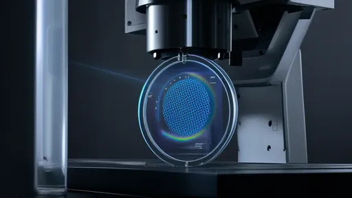
The realm of quantum-level defect detection has entered uncharted territory with the advent of photon-scanning nanoscale error analysis. This groundbreaking approach is redefining precision in materials science, semiconductor manufacturing, and photonics engineering. Unlike conventional microscopy or spectroscopy techniques, photon-scanning probes interact with subatomic particles to reveal imperfections invisible to other methodologies.
At the heart of this revolution lies the ability to detect lattice irregularities at resolutions below 0.1 nanometers. Traditional electron microscopy struggles to identify quantum-scale defects without altering the sample through electron bombardment. Photon scanning achieves non-destructive measurement by leveraging quantum entanglement principles, where probe photons become correlated with the sample's atomic structure. When these photons are later measured, they reveal information about the sample without direct interaction that could cause damage.
The implications for semiconductor fabrication are particularly profound. As chip manufacturers push toward 2nm and smaller process nodes, quantum defects that were previously negligible now threaten yield rates. Photon-based detection allows foundries to identify crystal vacancies, interstitial atoms, and dislocation loops that contribute to electron scattering. Early adopters report a 40% reduction in wafer rejection rates after implementing this quality control measure.
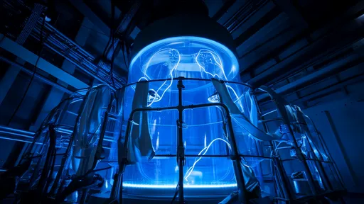
What makes this technology truly remarkable is its dual capability for both detection and correction. Advanced systems now incorporate femtosecond laser arrays that can perform atomic-scale repairs immediately following defect identification. This closed-loop system represents the first practical implementation of self-healing materials at the quantum level. The laser pulses are precisely tuned to the vibrational modes of specific atomic bonds, allowing for targeted restructuring without thermal damage to surrounding areas.
In photonic applications, the technique has exposed previously unknown scattering centers in optical fibers that contribute to signal loss. Telecom companies are using these insights to develop next-generation fibers with attenuation coefficients approaching the theoretical limit. The military sector has taken particular interest in applying this to quantum communication systems where even single-photon losses can compromise encryption protocols.
The methodology relies on a sophisticated apparatus combining quantum light sources, superconducting single-photon detectors, and AI-driven pattern recognition. The photon emitter generates entangled photon pairs - one interacts with the sample while the other serves as a reference. Superconducting detectors with timing resolutions below 10 picoseconds capture the interaction signatures, while machine learning algorithms distinguish between normal atomic variations and actual defects.
Recent breakthroughs have extended the technique's applicability beyond static samples. High-speed photon scanning can now capture defect dynamics in operating semiconductor devices, revealing how quantum imperfections evolve under electrical stress. This has led to the discovery of previously unknown failure mechanisms in advanced node transistors. Researchers observed that certain atomic vacancies actually migrate under applied voltage, creating transient conductive paths that lead to eventual device failure.
The scientific community anticipates this technology will accelerate materials discovery through high-throughput quantum defect characterization. Several national laboratories are establishing photon-scanning facilities to screen candidate materials for fusion reactors, quantum computers, and next-generation batteries. By identifying and quantifying defect types at unprecedented scales, researchers can establish clearer structure-property relationships that guide materials design.
Commercial implementation faces challenges, particularly regarding equipment costs and operational complexity. Current photon-scanning systems require cryogenic cooling and vibration isolation approaching laboratory standards. However, several startups are working on compact, field-deployable versions using novel room-temperature quantum sensors. Industry analysts predict the market for quantum defect detection tools will exceed $2.7 billion by 2028 as the technology matures.
Ethical considerations have emerged regarding potential military applications. The same techniques that improve civilian technology could also enhance nuclear weapons monitoring or stealth material development. Scientific organizations are establishing guidelines for responsible knowledge sharing while maintaining necessary security protocols. This balancing act will likely define the technology's dissemination in coming years.
Looking ahead, researchers envision combining photon-scanning with quantum computing to simulate defect formation in real-time. Such capability would enable predictive maintenance at the atomic scale, potentially extending device lifetimes by orders of magnitude. As the boundary between measurement and manipulation blurs, we stand at the threshold of a new era in precision engineering - one where quantum imperfections become not just detectable, but designable features.

By /Jul 25, 2025

By /Jul 25, 2025

By /Jul 25, 2025

By /Jul 25, 2025

By /Jul 25, 2025

By /Jul 25, 2025

By /Jul 25, 2025

By /Jul 25, 2025

By /Jul 25, 2025

By /Jul 25, 2025

By /Jul 25, 2025

By /Jul 25, 2025

By /Jul 25, 2025
By /Jul 25, 2025

By /Jul 25, 2025

By /Jul 25, 2025

By /Jul 25, 2025

By /Jul 25, 2025
By /Jul 25, 2025

By /Jul 25, 2025